- 您现在的位置:买卖IC网 > Sheet目录1990 > BU2363FV-E2 (Rohm Semiconductor)IC CLOCK GEN DVD-VIDEO SSOP-B16
BU2285FV,BU2363FV
Technical Note
13/16
www.rohm.com
2009.04 - Rev.A
2009 ROHM Co., Ltd. All rights reserved.
1:VDD1
24:CLK33M
33.8688MHz
0.1uF
2:VSS1
23:CTRLB
OPEN:27.0000MHz
L
:13.5000MHz
16.9344MHz
3:CLK16M
22:CLK54M
54.0000MHz
4:AVSS
21:OE
OPEN:Enable
0.1uF
L
:Disable
5:AVDD
20:CLKDAC
27.0000MHz
or 13.5000MHz
6:AVDD
19:DVDD
0.1uF
7:AVSS
18:DVSS
8:XTALIN
17:DVSS
9:XTALOUT
16:CLK27M
27.0000MHz
10:NC
15:VDD2
OPEN:48.0kHz type
0.1uF
L
:44.1kHz type
11:CTRLA
14:VSS2
36.8640MHz
12:CLKA
13:CLKB
18.4320MHz
or 33.8688MHz
or 16.9344MHz
BU2285FV
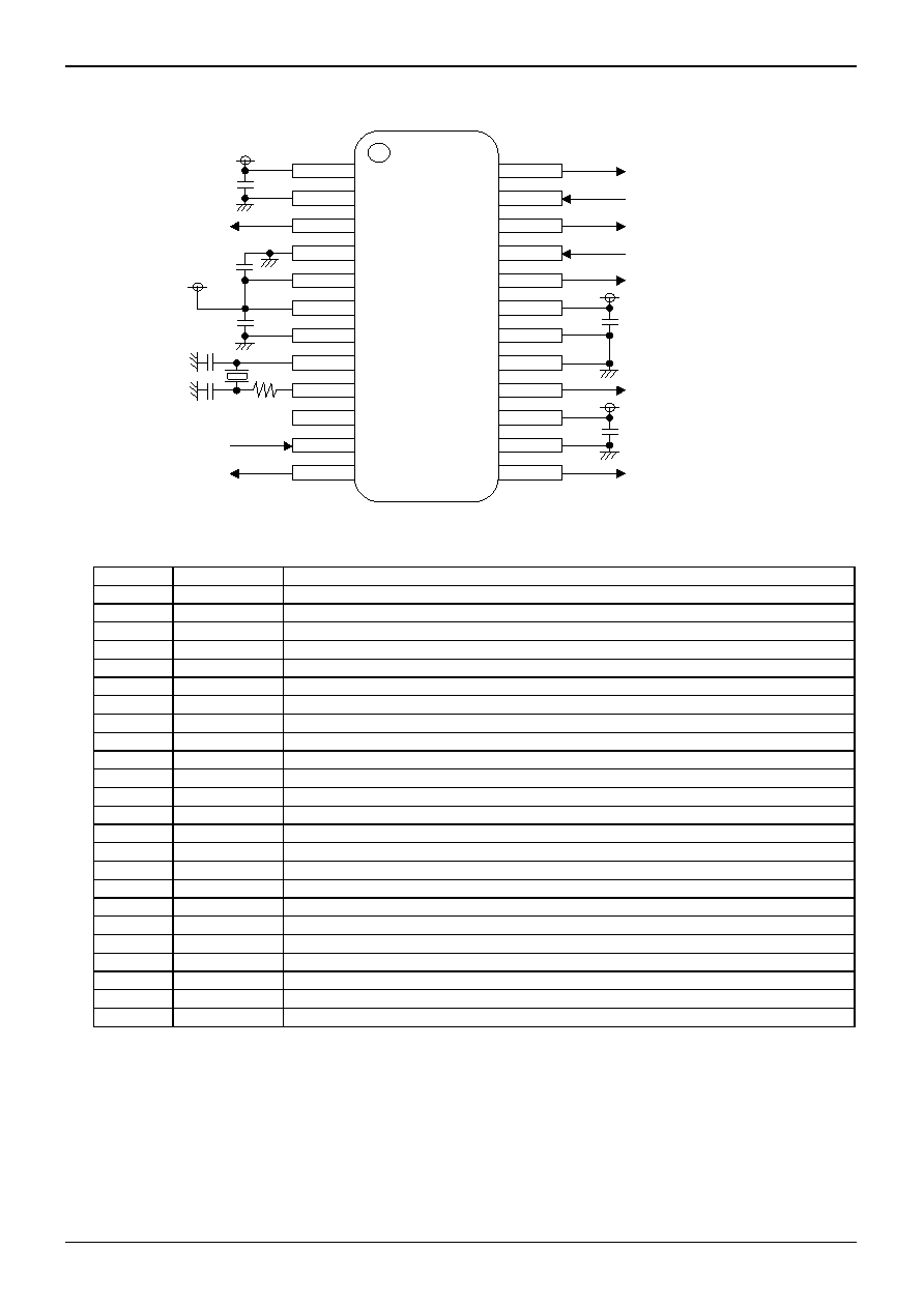
●Example of application circuit
◎BU2285FV
Pin Function
PIN No.
PIN Name
PIN Function
1
VDD1
33MHz system power supply
2
VSS1
33MHz system GND
3
CLK16M
16.9344MHz output
4
AVSS
Analog GND
5
AVDD
Analog power supply
6
AVDD
Analog power supply
7
AVSS
Analog GND
8
XTALIN
Crystal input terminal
9
XTALOUT
Crystal output terminal
10
NC
11
CTRLA
CLKA or B output selection (with pull-up)
12
CLKA
CTRLA=OPEN:36.8640MHz, CTRLA=L:33.8688MHz
13
CLKB
CTRLA=OPEN:18.4320MHz, CTRLA=L:16.9344MHz
14
VSS2
CLKA, B
GND
15
VDD2
CLKA, B
power supply
16
CLK27M
27.0000MHz output
17
DVSS
Digital GND
18
DVSS
Digital GND
19
DVDD
Digital power supply
20
CLKDAC
CTRLB=OPEN:27.0000MHz, CTRLB=L:13.5000MHz
21
OE
Output enable (with pull-up), OPEN:enable, L:disable
22
CLK54M
54.0000MHz output
23
CTRLB
CLKDAC output selection(with pull-up)
24
CLK33M
33.8688MHz output
Note) Basically, mount ICs to the printed circuit board for use.
(If the ICs are not mounted to the printed circuit board, the characteristics of ICs may not be fully demonstrated.)
Mount 0.1
F capacitors in the vicinity of the IC PINs between 1PIN (VDD1) and 2PIN (VSS1), 4PIN (AVSS) and 5PIN (AVDD), 6PIN (AVDD) and 7PIN
(AVSS), 14PIN (VSS2) and 15PIN (VDD2), and 17PIN/18PIN (DVSS) and 19PIN (DVDD), respectively.
Depending on the conditions of the printed circuit board, mount an additional electrolytic capacitor between the power supply and GND terminal.
For EMI protection, it is effective to put ferrite beads in the origin of power supply to be fed to BU2285FV from the printed circuit board or to insert a
capacitor (of 1
or less), which bypasses high frequency desired, between the power supply and the GND terminal.
Fig.85
发布紧急采购,3分钟左右您将得到回复。
相关PDF资料
BU2365FV-E2
IC CLOCK GEN W/VCXO SSOP-B24
BU2505FV-E2
IC DAC 10BIT 10-CHAN SSOP-B20
BU2508FV-E2
IC DAC 10BIT 4-CHAN SSOP14
BU3076HFV-TR
IC CLOCK GEN 1CH HVSOF6
CA3338AMZ96
IC DAC 8BIT 50MSPS R-R 16-SOIC
CDCR83DBQG4
IC DIRECT RAMBUS CLK GEN 24-QSOP
CDP68HC68T1M
IC RTC 32X8 NVSRAM CMOS 20-SOIC
CPLL66-1600-2200
IC VCO PLL/SYNTH 2.2GHZ SMD
相关代理商/技术参数
BU2363FVFV-E2
制造商:ROHM 制造商全称:Rohm 功能描述:DVD-Audio Reference Clock Generator for Audio/Video Appliance
BU2365F-E2V
制造商:ROHM 制造商全称:Rohm 功能描述:Clock Generator with Built-in VCXO for Audio/Video Equipments
BU2365FV
制造商:ROHM 制造商全称:Rohm 功能描述:Clock Generator With Built-in VCXO
BU2365FV_08
制造商:ROHM 制造商全称:Rohm 功能描述:Clock Generator with Built-in VCXO for Audio/Video Equipments
BU2365FV-E2
功能描述:时钟发生器及支持产品 CLOCK GEN W/VCXO A/V EQUIPMT RoHS:否 制造商:Silicon Labs 类型:Clock Generators 最大输入频率:14.318 MHz 最大输出频率:166 MHz 输出端数量:16 占空比 - 最大:55 % 工作电源电压:3.3 V 工作电源电流:1 mA 最大工作温度:+ 85 C 安装风格:SMD/SMT 封装 / 箱体:QFN-56
BU2370FV
制造商:ROHM 制造商全称:Rohm 功能描述:VCO + phase comparator for TV
BU2373FV
制造商:ROHM 制造商全称:Rohm 功能描述:VCO & Phase-Detector for PLL System
BU2373FV_11
制造商:ROHM 制造商全称:Rohm 功能描述:High Performance VCOs for Image Sampling